The graphene-info newsletter (February 2014)
Published: Mon, 02/03/14


Samsung invests in XG-Sciences |
XG Sciences announced that Samsung Ventures placed a strategic investment in the company. We do not know the financial terms, but XGS said they plan to formalize their development work with Samsung SDI (the world's largest Li-Ion battery maker) in a joint development program aimed at next-generation batteries for consumer electronics and other devices.
In April 2013 XG Sciences launched new graphene-based anode materials for Li-Ion batteries that has four times the capacity of conventional anodes. The new anode materials use the XG's xGnP graphene nanoplatelets to stabilize silicon particles in a nano-engineered composite structure. Later in November 201 XGS has been awarded $1 million in funding from the US Department of Energy for continued development of these lithium-ion battery materials. It is not clear whether these materials are part of the development effort of XGS and Samsung SDI. In July 2013, we published an interview with Mike Knox, XG Sciences' co-founder and CEO.
IBM researchers make the world's most advanced G-FET IC |
IBM researchers built a graphene (GFET) based radio frequency receiver IC which they say is the world's most advanced IC ever made of graphene - in fact it offers 10,000 times better performance and any previously reported effort.
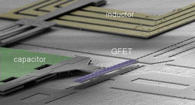
IBM's circuit consists of three graphene transistors, four inductors, two capacitors, and two resistors. All circuit components are fully integrated into a 0.6 mm2 area and fabricated in a 200 mm silicon production line. The researchers say that those the circuits consume less than 20 mW power to operate, while also demonstrating the highest conversion gain of any graphene RF circuits at multiple GHz frequency.
IBM already built an analog graphene integrated circuit with a broadband frequency mixer in a 2011, but that device suffered from poor performance due to harsh fabrication processes. For this new IC, the research team completely reversed the conventional silicon integrated circuit fabrication flow, leaving graphene transistors as the last step of integrated circuit fabrication. This resulted in preserving graphene device performance.
Pencil and paper used to create sensors |
Students from Northwestern University managed to use pencils and regular paper to create functional sensor devices. They created two types of sensors - strain sensors and chemical vapor sensors.
The students realized that when you draw a line on a piece of paper with a pencil, the pencil's graphite sheds numerous graphene sheets. They started exploring what these graphene sheets can be used for, and managed to create two simple sensors. You can read more about this interesting research here.
BASF and NUS to develop graphene for OLEDs and OPVs |
The Graphene Research Centre (GRC) at the National University of Singapore (NUS) and BASF announced a new partnership to develop the use of graphene in organic electronics devices - such as OLED devices. The goal of this collaboration is to interface graphene films with organic electronic materials, with an aim to create more efficient and flexible lighting devices.
The GRC will contribute its graphene knowledge (the synthesis and characterization of the graphene) while BASF is focused on organic materials. Of course BASF is also engaged with graphene research (for several years) and are looking to speed up their device development with this new partnership.
New graphene-like materials |
In the past month, three different new graphene-like materials were discovered. First up is Borophene, which is made from Boron. Boron has one fewer electron than carbon so it cannot form a honeycomb lattice. But now it turns out that you can make a cluster of 36 Boron atoms called B36 that looks like a disc with a hexagonal hole in the middle. This B36 can be used to form an extended planar 2D graphene-like material. Borophene is fully metallic and so may prove to be a better conductor than graphene - but it wasn't actually made yet.
The second material is made from phosphorus and is called Phosphorene. This is the first native 2D p-type semiconductor - which make it more useful than graphene to make transistors. Together with MoS2 (a 2D n-type semiconductor), it is now possible to build switches made from 2D materials. Graphene in its basic form is a superconductor and so is less suited to make transistors. Phosphorene was already produced and researchers are now studying it.
The last material is Stanene, a tin-based 2D material that may be the first material to conduct electricity with 100% efficiency at the temperatures that computer chips operate. Stanene is currently theoretical only, but hopefully experiments will soon confirm those predictions.
Top Graphene News |
The UK's FCA warns against graphene investment scams
Companies have approached investors offering them to buy graphene materials, and the UK's FCA warns against scams.
UCF to develop graphene-based spray
The University of Central Florida develops a polymer-graphene composite based spray that will be used to strengthen materials and protect them from corrosion. Garmor will assist with graphene-oxide formulation.
Cientifica and London Graphene to co-develop graphene for energy storage
Cientifica's first public deal is with London Graphene. The two companies will raise further funds to facilitate this plan.
CVD Equipment to lower CVD graphene production costs
CVD Equipment developed a new method to produce large-size high-quality CVD graphene in increased quantity and at a lower cost. CVD will ship those new systems in Q2 2014.
Mason Graphite acquires 40% of NanoXplore for $700,000
The Canadian graphite mining company acquired 40% in NanoXplore, an R&D company that develops a graphene production method.
GO-based skin cancer therapy
A new skin cancer photothermal therapy uses graphene oxide - the idea is to attach the GO particles to tumor cells, and then shine near-infrared laser light on them. The GO generate heat, destroys the tumor cells, while healthy cells are not effected
Graphenea slashes its graphene prices by 27%
Graphenea announced it reduced prices by around 27% due to increased production efficiency, an improvement in process yield, and the acquisition of new lab equipment
Send this to a friend |
Do you have a friend or a colleague that might be interested in Graphene technology? Forward this mail to update him on the
world of Graphene.
If you received this email from a friend, subscribe to this
newsletter here!