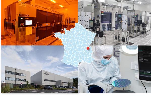
Photograph : Aledia’s own $200M production line in France for fast product development and mass production is a strong competitive advantage
What’s Next: Challenges Worth Solving
Despite progress, several challenges remain. Yield optimization at sub-10μm pixel sizes, long-term reliability testing, and integration with flexible backplanes are still works in progress across
the sector. Hybrid models such as miniLEDs or quantum dot–layered systems provide useful steppingstones but fall short of delivering the efficiency and precision of true microLEDs.
We are closely following the efforts of the MicroLED Industry Association to establish standards for wafer formats and system architectures, a critical step in avoiding market fragmentation. At Aledia, we are contributing to these discussions while advancing our roadmap, which includes automotive-grade
reliability testing, custom driver IC integration, and partnerships with OEMs in Europe, North America, and Asia.
The Stakes and the Payoff
What makes 2025 different is not only the technical maturity of microLED but also the alignment across the ecosystem. For the first time, display makers, chip manufacturers, and materials innovators are moving in unison toward the same goal.
As we look ahead to Touch Taiwan, and SID Display Week 2026, the industry is preparing for
the first wave of commercial microLED products. At Aledia, we are not just anticipating that future. We are building it now, pixel by pixel and wafer by wafer.