MicroLED-Info weekly newsletter
Published: Tue, 11/08/22

The MicroLED-Info newsletter (November 9, 2022)
Cannot read this? View it online here
MICLEDI announced a high-performance native-red GaN microLED device
Belgium-based microLED microdisplay developer MICLEDI has demonstrated 630nm wavelength red GaN with a full-width-half-max (FWHM) in the range of 50nm. New red microdisplay samples are projected to be available to customers before the end of the year.
MICLEDI says that its red GaN device is compatible with the company's proprietary CMOS-fab technology and it follows the identical process recipe of the company’s blue and green arrays for consistency. The new red device is tailored for 300 mm processes for high-volume mass production.
Just One Touch installs the world's first $800,000 219-inch Samsung The Wall residential microLED TV
An California-based integrator, Just One Touch/Video & Audio Center, announced that it has installed the first-ever residential installation of Samsung's latest 219-inch microLED The Wall TV. The price of this project was about $800,000. The installation took three days to complete.
The 219-inch display is made from the IW-008A modules, which offer a 0.84 mm pixel pitch, 120Hz refresh rate, a peak brightness of 2,000 nits and a maximum brightness of 250 nits.
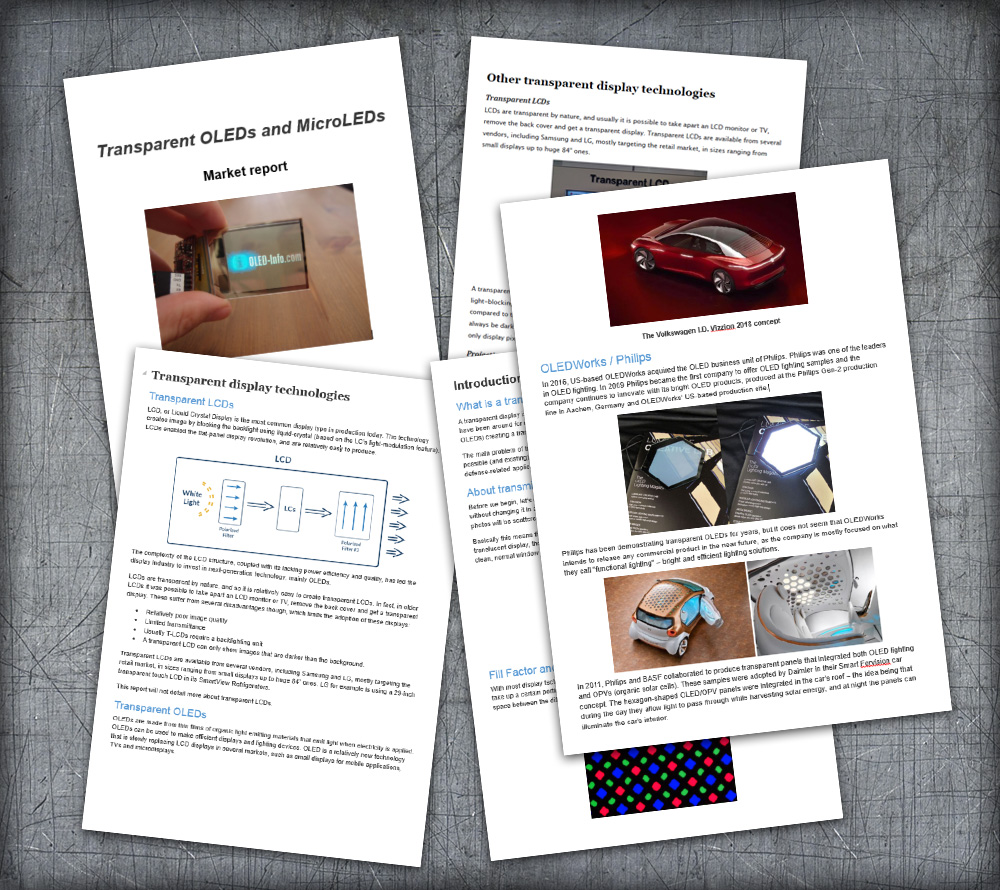
A new version of our Transparent MicroLED and OLED Market report released
Today we published a new edition of our Transparent MicroLED and OLED Market Report, with all the latest information. The new edition includes news from LG Display, BOE, LUMINEQ and OTI.
Reading this report, you'll learn all about:
- Transparent OLED and MicroLED properties and advantages
- The transparent OLED and MicroLED industry
- What kind of transparent OLEDs are currently on the market
- The transparent OLED lighting market
The report package also provides:
- Transparent OLED display product listing
- A guide into buying transparent OLEDs
- The main challenges towards transparent displays
- Free updates for a year
This transparent displays market report provides a great introduction to transparent OLED and MicroLED technologies and covers everything you need to know about the market and industry now and in the future. This is a great guide for anyone who's thinking about adopting transparent displays in their products or that wants to understand this industry and market throughout.
Kyoreca developed a new process to grow low-defect microLED GaN devices
Kyocera Corporation announced that it has successfully developed a new process technology to produce microLED (and micro-laser) devices. The process is based on lateral growth of GaN layer on a silicon wafer, in a way that limits defects in most of the area.
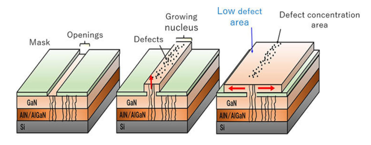
The basic process has three steps. First you grow a GaN layer on silicon. The second step is to apply a mask with a has a horizontal gap. The third step is to continue growing the GaN layer. The defects are concentrated in the opening nucleus, but the rest of the growth area remains almost defect free. The actual microLED devices are fabricated from the low-defect region.
Spotlight on ALLOS Semiconductors: a Microled Industry Association member
We're happy to interview ALLOS Semiconductors, as part of our new series of interviews with MicroLED Industry Association members. ALLOS Semiconductors is an IP licensing and technology company that focuses on GaN-on-Si technology for the microLED industry. ALLOS offers a turn-key technology transfer to establish a super-uniform CMOS-compatible large epiwafer process at customers within only 12 weeks.
Q: Hello! Can you introduce your company and technology?
ALLOS Semiconductors is the global leader for gallium nitride on silicon epiwafer technologies (GaN-on-Si) for next generation, micro LED-based display solutions and other applications building on more than 20 years track-record.
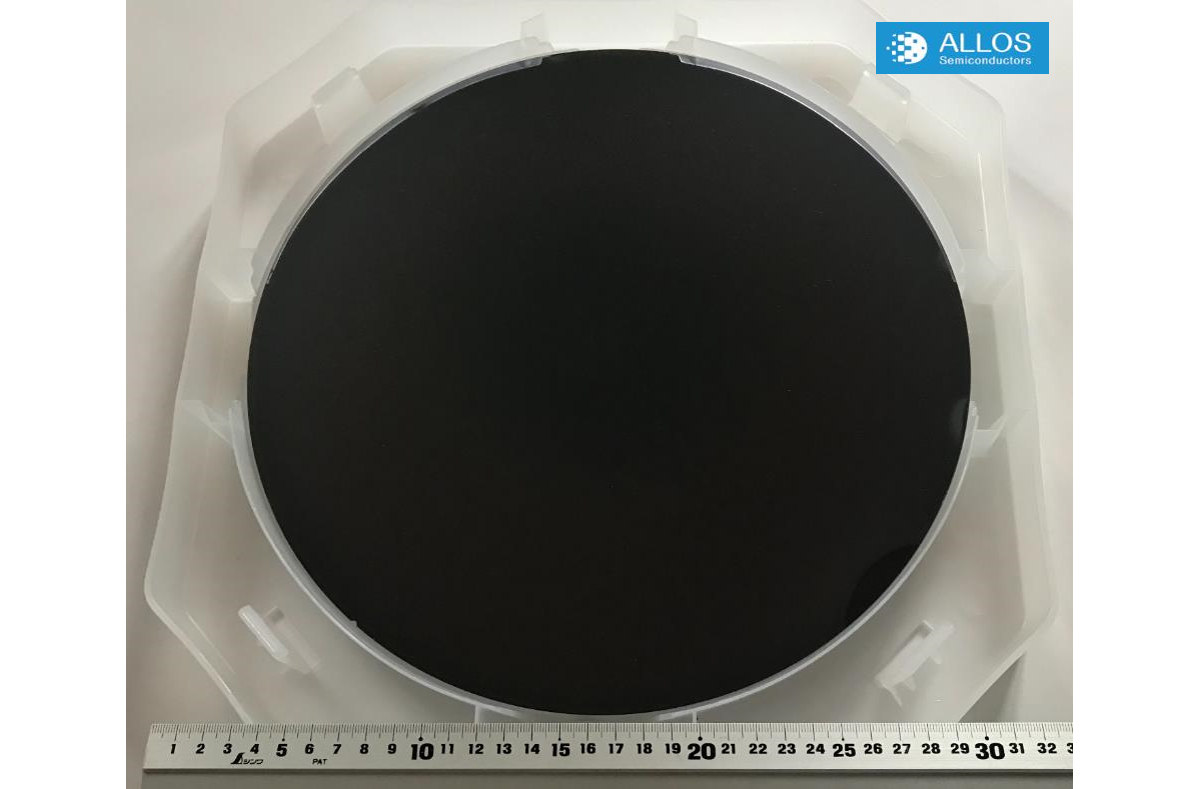
Our customer and partner base includes top-tier companies from the electronic device, display, LED and semiconductor foundry industries. They benefit from the cost, yield and performance advantages of our patent-protected 200 and 300 mm GaN-on-Si micro LED epiwafer technologies – including our unique 1 bin® technologies.
Q: Can you say why you joined the microLED association and what it is you hope to achieve?
Micro LED displays are poised to deliver huge benefits. However, competition from LCD and OLED competitors is fierce. The association can strengthen the dialogue within the industry in order to accelerate adoption and success of micro LEDs in the market. Tasks include facilitating cooperation, developing standards and engaging into dialogues with the public and all stakeholders.
Q: What is your biggest challenge, and success to date in the microLED industry?
We see four fundamental challenges – which also differentiate micro LED from conventional or mini LEDs:
- Overcoming the tremendous yield challenge by using the manufacturing excellence of advanced 200 mm and 300 mm semiconductor fabs. ALLOS works with customers and partners to enable access to such manufacturing excellence for the micro LED industry.
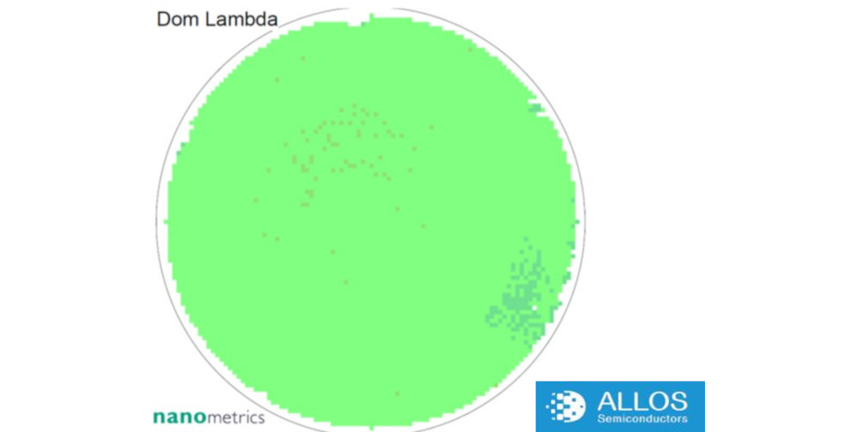
- Provide 200 mm and 300 mm GaN-on-Si epiwafers which can be processed in advanced semiconductor fabs. ALLOS is meeting those requirements; most importantly low bow, no cracks, no contamination and 725 / 775 µm thickness.
- Achieve single-bin quality for all required parameters to avoid costly sorting, testing and repair. Most important is achieving uniform colors. Here, ALLOS is already delivering up to 98.6 % of the epiwafer area in the target bin.
- Further improve and apply the various approaches to achieve RGB colors in an economic way. Most-likely different approaches like color conversion, red nitride and color-adaptable LEDs will co-exist. ALLOS works with customers and partners with diverse strategies and our platform supports all approaches.
Q: Can you detail your latest prototype/demonstration?
We constantly demonstrate improved generations of our 200 and 300 mm micro LED epiwafer technologies. We also work closely with several lead customers and partners, shipping batches of epiwafers every month for them to develop and improve their display performance and manufacturability.
Q: How do you see microLEDs changing the display industry in the next 5-10 years?
To our believe micro LED based displays have the potential to disrupt the traditional display industry (PID, TV, laptops, automotive, smartphones, smartwatches, etc.) as well as taking such displays to new performance levels.
Additionally micro LEDs are enabling completely new and today unforeseen applications. Light field as well as MR and AR displays – including such futuristic but already successfully prototyped ones being built into contact lenses – are already providing an idea of how interaction between humans and machines will evolve in the future.
Furthermore, we see many non-display applications for micro LEDs in for example, medicine, opto-electronics and automotive.
Last but not least we expect the market for mini LEDs and for conventional LEDs to benefit from the manufacturing breakthroughs achieved on the path of taking micro LEDs into volume production.
Toray Research Center to host a MicroLED, OLED and QD technology webinar
In the next two weeks, Toray Research Center (TRC) is hosting online webinars focused on display technologies. TRC, who supplies technical analysis and support for R&D and manufacturing, invites you to attend the online lectures at no cost, to learn more about microLED, OLED and QD technologies.

The webinars include recorded presentations, which will be available online up until to November 22. You can register for the webinars here.
DSSC sees the microLED market growing to $1.3 billion in 2027, led by wearable displays and microdisplays
DSSC says that microLED display revenues will grow from around $40 million in 2023 to over $1.3 billion in 2027. While this is fast growth, it means that DSCC does not believe microLED will penetrate large display markets at least until 2028, and indeed the analysts say that lowering production costs will be necessary before microLEDs can become competitive against OLEDs and LCDs.

DSSC sees microLED microdisplay, produced using a monolithic process, taking up about 25% of the microLED display market. The largest segment for microdisplays will be smartwatches or wearable displays - as the low pixel size (relative to other display segments, at least) means that microLED technologies is relatively mature for that segment.
LG Display developed a 12" 100 PPI full-color stretchable microLED display
LG Display demonstrated a 12" 100 PPI (pixel pitch 40 um) full-color stretchable MicroLED display. The display can stretch up to 20% (to create a 14" display).
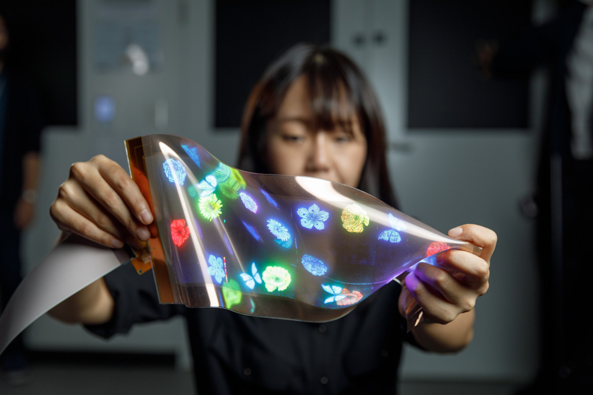
LGD says that this display can be commercialized soon, as it is highly flexible, durable, and reliable. The new display is produced on a "highly resilient film-type substrate made of special silicon used in contact lenses".
3D-Micromac sold several LLO systems for the production of microLED devices in Asia
3D-Micromac announced that a leading optical solutions provider has purchased several microMIRA laser lift-off (LLO) to use in the production of microLED devices. The systems will be installed in pilot lines and production lines at its state-of-the-art LED chip factory in Asia
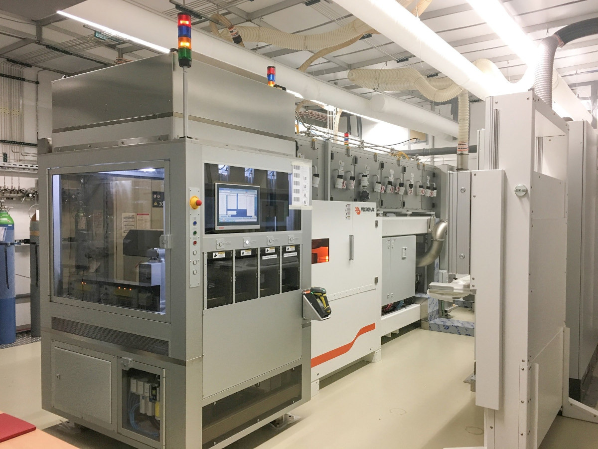
3D-Micromac says that the microMIRA laser system provides highly uniform, force-free lift-off of different layers on large-area substrates at high processing speeds without the need for costly and polluting wet chemical processes. The unique line beam system is built on a highly customizable platform that can incorporate different laser sources, wavelengths and beam paths to meet each customer's unique requirements. The system is capable of processing different substrate materials and sizes, and can achieve processing speeds (including handling) of up to 60 eight-inch wafers per hour.


Metalgrass LTD
9 Har Tsin St.
Kfar Sava Hasharon 4430809
ISRAEL
Unsubscribe | Change Subscriber Options